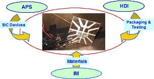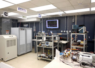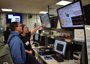
Fig. 1. A multidisciplinary team approach to developing technologies for high-temperature packaging of SiC devices.
Studies on wide band gap semiconductor devices, such as SiC or GaN diodes and transistors, have shown their great promise for revolutionizing the power electronics industry; their superior switching characteristics and ability to function at elevated temperatures up to 350°C reduce heat sink and cooling equipment requirements. However, interconnecting and packaging these devices for high-temperature uses pose a significant challenge. The state-of-the-art technology for interconnecting power devices typically involves attaching one terminal of the semiconductor die to a heat-sinking substrate with a lead or lead-free solder alloy or with an electrically conductive epoxy, while its other terminal(s) are generally attached by wire-bonding fine aluminum wires. Such interconnections are not able to function at the high temperatures of the wide band gap devices because of the low melting temperatures of solder alloys and low decomposition temperatures of epoxies and the susceptibility of aluminum wire to electromigration-induced failure at elevated temperatures.
To address the needs for high-temperature packaging of wide bandgap power semiconductor devices, CPES researchers from three thrusts pulled together their complimentary expertise in semiconductor devices, materials, and high-density packaging to work on the multidisciplinary problem. In this team effort as illustrated in figure to the left, researchers from the Advanced Power Semiconductors (APS) thrust contributed on SiC device design, fabrication, and characterization; Integratable Materials (IM) researchers applied their nanoscale silver paste with a low-temperature sintering technique to attach the SiC devices; and High-density Integration (HDI) researchers did the package fabrication and testing. Achievements of this joint project are important to systems-level advances as increasing levels of integration for power electronics modules in the test-beds present packaging challenges to accommodate increasing power density and operating temperatures.
