RESEARCH
Withstand Physics and Failure Mechanisms of p-Gate GaN HEMTs under Transient Surge Energy

GaN high-electron mobility transistors (HEMTs) has not been fully understood, as GaN HEMTs have no or very little avalanche capability. This work unveils the comprehensive physics associated with the surge-energy withstand process and failure mechanisms of p-gate GaN HEMTs in UIS tests.
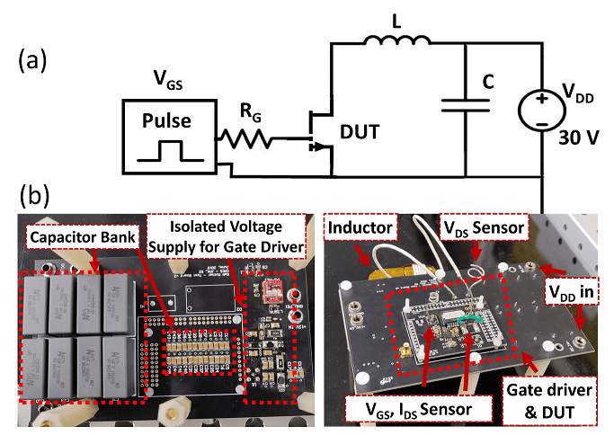
Fig. 1(a) and (b) show the UIS test circuit, during the test. The device-under-test (DUT) is first turned on to charge the inductor; once the current reaches the set value, DUT is turned off, and the energy stored in the inductor is forced to go through the DUT. Two types of devices were tested in this work: the 600 V, 31 A hybrid- drain gate injection transistor (HD-GIT) from Infineon and the 650 V, 30 A Schottky p-gate HEMT (SP-HEMTs) from GaN Systems. Fig. 2 (a) and (b) show the safe withstand waveforms; both devices show similar energy withstand process and show no degradation after the test. Four main phases are identified over the entire safe-withstanding process: Phase I: The device under test (DUT) is on and the inductor charged by VDD. Phase II: the DUT turns off, and its VDS exceeds VDD. Phase III: LC-like resonance between the load inductor (L) and the device output capacitance (COSS). Phase IV: once VDS resonates to negative values and exceeds the DUTâs reverse turn-on voltage, the DUT conducts in the third quadrant, and the LC-resonance ends. VDS is then clamped around its third-quadrant voltage drop, and the inductor is discharged by the power supply.
Fig. 2(c) and (d) show the typical failure waveform of the GIT and the SP-HEMT. In both types of devices, the failure occurs at the transient of peak-resonant voltage, which is around 1,150 V for GIT and 1,400 V for SP-HEMT. The failure modes exhibited in two devices are slightly different. In the GIT, a small collapse in VDS is shown after the device failure, indicating the leakage between drain and source. However, the gate control over IDS retains, and the resonance continues. In the SP-HEMT, the gate control is lost right after the device failure; the gate and source are short. To further study if the device failure depends on the duration of surge voltage, we performed the UIS tests with different inductors, which result in different resonance periods and durations of surge voltage. The results show that the maximum voltage VM that leads to device failure shows little dependence on the inductor values for both GITs and SP-HEMTs. This suggests that the device failure is almost solely limited by the device overvoltage capability or the transient physical BV. To conclude this work, the P-gate GaN HEMT transient surge energy capability is the same as the transient overvoltage capability.


